
Why I Write About Certified Soldering Repair
I am a certified soldering technician years repairing a wide range of electronics. Certification matters to my clients because it guarantees safety, traceability, and results.
I share practical best practices: workstation setup and ESD; tools, solder, flux, and consumables; through-hole and surface-mount techniques; diagnosing failures and advanced repair; QA, documentation, and customer communication.


The Value of Certification: Trust, Safety, and Compliance
What certification means in practice
For me, certification is documented training (IPC J-STD-001, IPC-A-610), proven competency, and routine equipment calibration. It’s the difference between “it worked” and “I can prove it was done to standard.”
Why it reduces risk
Certification enforces safe handling of fluxes and lead-free alloys, proper ESD control, and adherence to warranty or regulatory rules (RoHS/WEEE). Practical tips I use immediately:
Real-world payoff
I once avoided a $1,200 mainboard replacement by applying the correct lead-free profile learned in certification — a direct trust-builder with that customer and our partners.
Setting Up a Professional Workstation and Managing ESD
Ergonomics and bench layout
I arrange my bench so tools, microscope, and reels are within a smooth arc; an adjustable chair and 1,000–2,000 lux LED task lamp reduce fatigue. Parts bins are labeled and I physically separate leaded and lead-free jobs.
Lighting and fume extraction
I use a flexible LED lamp with color-corrected output and a local extraction arm for short-path capture; clear sightlines make repeatable soldering faster.
ESD control
Simple routines
I wipe mats with IPA, replace extractor filters per hours used, and restock tips and fluxes weekly to avoid contamination.
Choosing Tools, Solder, Flux, and Consumables Wisely
Tools I pick by task
I favor temperature?controlled irons (Hakko FX?888D or Metcal for heavy SMD), an Amscope stereo microscope or Dino?Lite USB for inspection, and precision tweezers (Dumont 5A). For rework I use a dedicated hot?air station.
Solder and flux choices
I choose Sn63Pb37 for repairs where allowed—easier wetting and lower temps—or SAC305 for RoHS jobs. No?clean flux pens for touch?ups, water?soluble for heavy rework, and Kester?style paste in syringes for BGA/tiny QFP.
Consumables & maintenance
Clean tips on brass wool, tin with tip tinner, calibrate irons monthly with a thermocouple, and replace consumables when:
Soldering Techniques I Rely On: From Through-Hole to Surface-Mount
Core principles
I focus on wetting, heat balance, sensible soldering order, and minimizing thermal stress. Proper wetting means clean metallization and the right flux; heat balance is using just enough energy to flow solder without cooking the board. In one repair I avoided a PCB delam by tacking pins quickly instead of brute?forcing heat.
Through?hole and SMT tactics
For through?hole I anchor corner or mechanical pins first, then finish signal pins. For SMT I tack opposite corners, use fine?point tweezers, and finish with short, decisive heats to avoid tombstoning.

Delicate parts, preheat & reflow
I preheat (80–120°C) when warming large copper pours, use thermal sinks (clips) on heat?sensitive leads, and prefer controlled reflow or hot?air for fine?pitch ICs.
Diagnosing Failures and Applying Advanced Repair Methods
Troubleshooting workflow
I start with visual inspection under an Amscope microscope, then use thermal imaging (FLIR C5) to spot hot spots. I follow with continuity checks (Fluke 87V) and in?circuit tests, finishing with signal tracing using a Siglent SDS1000X or a handheld probe.
Stepwise checklist
Repair decision logic
I weigh board cost, failure mode, and downtime: component?level swap when pads are intact; board?level repair or donor swap when land damage or multi?layer faults exist.
Advanced methods & precautions
I reball BGAs with stencils and Quick 861DW hot?air, rebuild micro?SMT nets with micro?wires and conductive epoxy, and reconstruct traces with copper tape and epoxy. I use thermal clamps, minimal heat, and extended soak tests to verify long?term reliability before moving to QA.
Quality Assurance, Documentation, and Customer Communication
QA steps
I run a strict sequence: visual inspection under magnification, functional testing in real operating conditions, and burn?in (4–24 hours) when the failure or component warrants it. I verify against acceptance criteria I record up front — voltages, signal integrity, thermal stability — and log any deviations.
Documentation I deliver
Communicating with customers
I explain residual risks, realistic lifetimes (e.g., electrolytic caps vs ceramic MLCCs), and simple maintenance steps so expectations align before handoff. These practices set the stage for the concluding lessons.
Lessons That Guide My Certified Soldering Practice
I learned certification builds trust and enforces safety and compliance; disciplined setup, ESD control, and thoughtful tool and consumable choices make repairs predictable.
Thorough testing, clear documentation, and honest communication protect the device and client. I encourage prioritizing certified, standards-based repair to achieve consistently reliable outcomes. Quality and accountability start with certified skills.
This was helpful, but I kept waiting for a deeper dive on solder alloys and flux choices.
– The article mentions choosing solder/flux wisely, but is the author recommending leaded for rework or sticking with lead-free for cert compliance?
– Any favorite flux brands for stubborn oxidized pads?
– Also, can someone recommend soldering iron tips for the YIHUA 926 III that last? I burn through tips too quickly.
Thanks — I’m trying to standardize our shop supplies and would love some practical recs.
Good questions, Maya. Short answers:
– Certification often allows leaded solder for repair if local regs permit, but many shops standardize on lead-free for consistency and customer expectation.
– For flux: no-clean rosins for general work, and a more active RMA or water-soluble flux for tough oxidized joints (with proper cleaning).
– For YIHUA 926 III tips: choose nickel-plated copper tips from reputable vendors and avoid overdoing the temp — oxidation kills them faster. I’ll add a recommended-parts list to the article.
For flux, try a syringe of ‘no-clean’ for prototypes, and a jar of water-soluble for full restorations. Also, fwiw, deoxidizer + brushing helps a lot before soldering.
I got a tip set labeled ‘compatible with YIHUA 926’ on Amazon — cheaper ones last maybe 1/3 the time of branded tips. Spend a little more, you’ll save money and frustration.
If you can, keep a stash of leaded for reflow or delicate joints — the wetting is just better. Of course, label everything and get customer consent where required.
Also adding: always log which alloy you used in your QA docs — traceability is huge when customers ask later.
Solid write-up. I appreciated the section on QA docs. One thing I like to record is the tip number used on the iron and approximate hours on the tip before replacement.
Okay, full disclosure: I once ruined a board because I set the hot air way too hot and melted a nearby component. ?
The article’s reminder to practice temperature control (and use the right nozzle size on the YIHUA 959D) hit home. Also — if you’re doing tiny SMD work, invest in a proper set of tweezers and a fine tip iron. Cheap shortcuts cost more later.
PS: anyone else weirdly enjoy the sound of a soldering iron warming up?
I use low-temp profiles for plastics nearby — less heat soak and fewer oops moments.
Been there — thermal profile matters. I’ll add recommended temp/nozzle ranges for common component sizes as a quick reference.
And magnetic tweezers are life-savers for tiny chips. Seriously, get the nice ones.
Haha yes, I call it the ‘shop espresso machine’. Also, preheating the board helps reduce the time you need the hot air gun on a spot.
Constructive feedback: loved the techniques section, but could use more on when to escalate to advanced repair (BGA reball, micro soldering) vs. when to recommend replacement.
Also: shoutout to the 60W Adjustable Temperature Soldering Iron Kit listed — good starter kit but don’t expect miracles on tiny QFPs.
Anyone here certified and willing to share how long their certification took and what practical skills they found hardest?
I found the hands-on rework exercises the most valuable. Theory helps, but muscle memory on the iron and hot air is key.
For me, the intermittent fault diagnosis was the toughest — you need patience and methodical logging. A thermal camera helps sometimes too.
Good question, Fiona. Certification timelines vary, but most programs are a few days of hands-on plus coursework. Hardest skills usually: fine-pitch SMD soldering and diagnosing intermittent faults.
Minor nit: the section on diagnosing failures was great but threw a lot at newer folks quickly. Maybe a flowchart? Otherwise excellent tips.
Good point — a diagnosis flowchart is on my to-do list. I’ll try to simplify the troubleshooting steps and add visuals next edit.
Nice article. The workstation setup tips were the most practical for me — especially the ESD mat placement and wrist strap grounding.
Quick Q: anyone had issues with the KOTTO extractor being noisy? I love the filter but it sounds like a vacuum cleaner.
Noted — I’ll include a short section on extractor placement and noise mitigation (short flexible ducting, rubber feet, and using lower fan speeds when possible).
It’s a bit loud, yep. I put it a little farther away and duct the suction with a flexible arm — works fine, still hears some motor hum though.
Short note: the YIHUA 959D hot air station mentioned is a solid piece of kit for removing SMDs — tip control matters more than you think. Also the article’s emphasis on safety/compliance is on point.
Long-ish thought — I really appreciated the part about customer communication and documentation.
Most shops forget that customers just want confidence: a clear before/after photo, an explanation of what failed, and a simple note about longevity expectations.
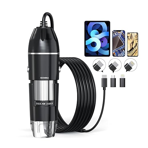
Practical tip: use the Handheld USB Digital Microscope for high-res before/after pics. 50x for the whole area, 400x for the joint.
Also, the YIHUA 939D+ pairs great with a KOTTO extractor for small board reworks.
Also add a short layman summary line for customers who don’t want tech details. ‘Replaced bad solder joint — device tested OK.’ Simple.
Exactly the mindset we try to teach in certification — transparency builds trust. Thanks for sharing your photo workflow, Hannah.
I’ll publish a simple photo-template that cert holders can reuse — before, during, after, and test results included.
Pro tip: stitch multiple microscope shots into a single image for the report so customers can zoom without seeing too many tiny files.
And keep a folder per customer. My shop’s saved us more than once when warranty questions pop up months later.
I label photos with timestamps and a short note (‘cold joint’, ‘reflowed’, etc.). Makes QA reports look pro and reduces follow-up questions.
Great read — love the focus on certification and traceability. The bit about documenting repairs really resonated with me.
I personally use the YIHUA 939D+ for heavier jobs and the KOTTO fume extractor nearby — saved my coworkers from a headache (literally). ?
Would be nice to see a short checklist for incoming repairs though (what to test first, what to photograph).
Totally agree about the checklist. Also, anyone tried using the handheld USB microscope for pre/post photos? I find 200x is usually enough for solder joints.
I use the microscope at 400x for tiny BGA reballs — night and day difference. But for customer pics, 50–100x looks less scary and more useful.
Thanks Emily — good suggestion. I’ll add a short incoming-inspection checklist to the next update: photo angles, power-on checks, and ESD contact points to record.