Why Etch a PCB at Home?
I’ll show you how to etch a PCB at home safely and affordably, using simple tools and common chemicals so you can prototype quickly and confidently right now.
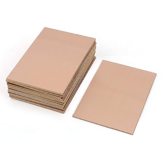
Materials, Tools, and Skills I Use
I use copper-clad board, laser toner or photoresist, etchant, PPE, trays, drill, heat source.

Design and Prepare Your PCB Artwork
Why spend hours drawing when I can have a laser copy ready in minutes? Prepare like a pro to avoid etching mistakes.Design the circuit in my favored PCB CAD; I check dimensions, trace widths (e.g., 10 mil for hand routing), and drill holes. Print the artwork mirrored on glossy laser paper or prepare a photoresist film.
Trim the copper board slightly larger and clean it with an abrasive pad and isopropyl alcohol so the toner/photoresist adheres. Align the artwork precisely so traces land exactly where I expect.
Transfer the Toner or Expose the Photoresist
Will a clothes iron or my laminator really save me money? Yes—if I follow the steps.Place the printed artwork face down on the cleaned copper.
I use a hot iron or laminator and apply steady pressure and heat to bond the toner.
Expose the photoresist to UV with the film flat, then develop per instructions.
Check for missing traces; I touch up gaps with nail polish or a permanent marker before etching.

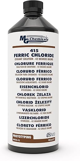
Etch the Board Safely and Efficiently
Is this the smelly, dangerous part? Not when I use simple safety rules and a controlled process.Mix the etchant per product instructions; I follow concentration and temperature guidelines.
Wear chemical-resistant gloves and goggles and work in a ventilated area.
Pour the solution into a plastic tray and submerge the board. Agitate gently — I tilt the tray or stir with a plastic spatula every 30 seconds — and monitor progress. Stop once unwanted copper is gone, then rinse thoroughly.

Remove Toner, Clean, and Inspect
Clean-up reveals the truth—will my traces be perfect? I look for flaws and fix them now.Remove the toner or resist with acetone or an appropriate stripper; I wipe with a cotton pad until copper shows.
Inspect under magnification; I use a 10× loupe to find undercuts, bridges, or gaps.
Clean pads with a fiberglass pen or fine sandpaper and remove burrs.
Repair by soldering tiny bridges or applying conductive ink for gaps. I once fixed a bridged trace by soldering.
Rinse, dry, and verify continuity with a multimeter before drilling and assembly.
Drill, Solder, and Test Your Finished PCB
Will this actually work in a real circuit? I’m testing live to find out fast.Mark hole centers; I use a felt-tip and a center punch. Drill component holes carefully with the correct bit sizes, clean burs, and choose whether to apply solder mask or leave bare pads. Populate parts observing polarity and footprint, solder with a steady hand, and trim leads.

Ready to Prototype
I’ve taken you from idea to tested board in five steps; with care, patience, and safety I prototype reliable PCBs at home. Try it, iterate, and share your results today.
Awesome guide — thanks for laying this out so clearly!
I tried a home etch last month and your Step 3 on etching safely is spot on. A couple notes from my own trial:
– Use a plastic tote to contain splashback when agitating the etchant.
– Keep a digital thermometer nearby; temps make a huge difference in etch time.
Also, Step 2 (toner transfer) took me like 4 tries before I got the heat and pressure right. Don’t give up — practice makes perfect. ?
I can confirm the temp thing — I switched to slightly warmer etchant and my etch times halved. Also, putting a small fan on low helps reduce fumes in the workspace.
Totally agree on the multiple tries. I started by using glossy magazine paper (so bad) and then switched to proper transfer paper — game changer.
Thanks for sharing these practical tips, Emma — the tote suggestion is great (keeps the mess contained). If you’re open to sharing, what transfer press/iron settings worked best for you? Might help readers replicate your success.
I’m kinda on the fence about doing this at home. Safety-wise, the etchant fumes and waste disposal seem scary. The guide touches on safety but could use more specifics on PPE and disposal rules (at least mention neutralization or hazardous waste drop-off).
Also, drilling tiny vias at home? My Dremel vibes are terrible and I wrecked a board trying to center a bit. Any recs for affordable drill stands or guides?
Valid concerns, Clara. We should have expanded the safety section — PPE: chemical-resistant gloves (nitrile), eye protection, and a respirator rated for acid/metal fumes if you’re doing lots of boards indoors. For disposal: do not pour etchant down the drain — follow local hazardous waste procedures or neutralize with sodium carbonate and recover copper per local regulations. For drilling, a simple drill press or a Dremel drill press attachment makes a huge difference for alignment and vibration control.
Agree with admin. For DIYers, a cheap bench drill from a garage sale is worth it. Clamps + sacrificial spoil board = much better control. And yeah, never pour used ferric chloride down the sink!
Nice concise guide! I wanted to add a couple of practical hints for Step 4 and Step 5:
1) After etching, use acetone to remove toner but test a tiny spot first — some boards/discoloration can occur.
2) For drilling, get a bunch of 0.8, 1.0, and 1.2 mm bits — cheap kits on Amazon work fine. Keep bits sharp and replace often; dull bits wander.
3) When soldering, pre-tinning pads and using flux really speeds up assembly.
Hope that helps other beginners!
Thanks for the drilling and soldering tips, Sofia — pre-tinning and flux are underrated for hobbyists. I’ll incorporate these into a quick updates section.
Foam block storage is genius, Tom. I do the same now and it’s saved me from buying more bits!
Agree about the drill bits — I also store them in a foam block; keeps them aligned and you don’t accidentally snap the tiny ones.
This is great if you like chemical baths and patience. Me? I tried it once because I’m stubborn and apparently enjoy suffering ?. Biggest laugh was me etching the wrong side of the board — traced the foil pattern mirrored and had to start over. Noob move.
Also, pro tip: label your sheets. Seriously. Save yourself the shame.
Hahaha, Michael — been there too. I now always print a small ‘TOP’ arrow on the edge just in case.
I once etched an empty rectangle because I forgot to print the traces onto the transfer paper. Silence was my companion that day.
Been there — mirror errors are classic. I keep a checklist pinned up for each board: artwork orientation, transfer method, exposure time, etchant type. Saves a lot of facepalms.
LOL, these stories are golden. Cheers for the checklist idea, admin — adding it to my ritual.
If anyone wants, I can upload a simple printable checklist (artwork, mirror check, transfer, exposure, etch, clean, drill) — just say the word.
Good read. Quick question: in Step 2 you mention exposing photoresist — what exposure times are typical for UV LEDs vs sunlight? I tried sunlight once and it was inconsistent (clouds messed me up).
Also, you might want to mention the risk of underexpose/overexpose — I ruined a board by overexposing and couldn’t get traces to develop properly. Little tip: mark your first few exposure attempts with times so you can iterate.
Thanks — I’ll try test strips next time. Didn’t know about the datasheet detail, nice tip.
Great question, Raj. Exposure varies a lot by resin and light intensity. Rough ballpark: a 6W/cm² UV LED panel might need ~30–60s depending on resist; direct sunlight can be 10–60s but wildly variable. We recommend test strips (small square with different times) to dial it in. Always document each attempt so you don’t repeat mistakes.
If you’re using presensitized boards, the manufacturer sometimes lists exposure times on the datasheet. Saved me a headache once!
I do test strips too. Also, clouds are the worst — use a UV lamp if you want repeatable results. Sun is cheap but unpredictable.