Why I Build a BMS With You
I’ll guide you step-by-step as I design, build, and test a practical BMS, explaining decisions, trade-offs, and hands-on steps so you learn by doing safely and confidently every step.
What You Need Before We Start
Step 1 — Define Goals and Pick the Architecture
Want a safe, affordable, or high-performance pack? I’ll show how that choice drives everything.Define BMS goals: cell chemistry (e.g., 4S Li?ion), pack voltage, maximum charge/discharge currents (e.g., 60 A), and safety margins.
Choose topology: passive balancing, active balancing, or integrated IC; select monitoring ICs and a microcontroller. Plan connectors, shunt sizing, and thermal layout.
Validate these plans before committing to hardware.

Step 2 — Build the Power and Sensing Hardware
Soldering and layout decide whether this pack thrives or becomes a heated regret — here’s how I avoid mistakes.Assemble the power stage and sensing circuits on the PCB or protoboard; I solder shunts, MOSFETs, balance leads, and connectors.
Route high?current traces short and wide to minimize noise; I add decoupling capacitors and place temperature sensors adjacent to cells (for example, I tape an NTC to the negative terminal).
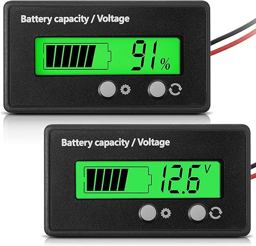
Implement per?cell voltage sensing and differential inputs where needed; wire the charger and external interfaces, fit the pack in an insulated enclosure, and clearly label terminals.

Step 3 — Develop Firmware and Control Algorithms
Want longer life and safer packs? I use simple tricks in firmware that punch above their weight.Write firmware that I use for cell monitoring, balancing control, and safety cutoffs. Implement ADC filtering and temperature compensation; for example, use an IIR filter on voltage samples and an NTC lookup table.
Add serial telemetry or a simple UI for live data and alarms. Tune PID balancing gains in simulation before bench testing. Include watchdogs, hardware failsafes, and OTA updates.

Step 4 — Test, Calibrate, and Harden for Safety
How do you prove a BMS is trustworthy? I break it first, then fix what breaks.Test the BMS with controlled charge/discharge using a programmable load and a reliable charger; I typically cycle at 0.5–1C (e.g., 5 A electronic load, 1C charger).
Verify balancing behavior; I measure temperature rise and calibrate ADC offsets and shunt values for accurate current sensing.

Wrap-Up and Next Steps
I summarize lessons learned, provide the full schematic, firmware links, and a troubleshooting checklist; try it, iterate, share your results, and please contact me for help — start building today now.
Loved the hands-on tone of this guide — felt like you were really at the bench with us.
A couple of things I tripped over: the section on sensing hardware didn’t mention isolation options for the current sensors, which can be a big deal when scaling to higher pack voltages.
Also, in Step 3 you reference an algorithm loop timing but don’t state target jitter/budget — would be great to see sample numbers.
Totally appreciated the safety-first focus in Step 4 though, that checklist was gold.
Thanks for laying this out so clearly, please keep the follow-up posts coming!
If you’re considering high pack voltages, opto-isolation or isolated sigma-delta ADCs saved me headaches. Also watch out for common-mode transients — they bite.
Agree on the jitter numbers — in my experience keeping the ADC trigger synchronized with the PWM edges reduces timing uncertainty a lot.
Great points, Sarah — thanks! I’ll add a short subsection on sensor isolation options (Hall vs. isolated shunts) in the next update and include recommended timing targets for the control loop (e.g., <1 ms jitter with 10 ms control period). Any particular pack voltage you're thinking of?
Haha, I expected this to be another fluffy blog post full of buzzwords, but nah — actual wiring diagrams? Bless you.
That said, minor troll mode: the ‘harden for safety’ section didn’t mention using a flame-retardant enclosure. Are we going to play with fire or what? ?
Seriously though, please cover thermal runaway propagation strategies and recommended spacing / venting. That’s the one thing that keeps me up at night when designing packs.
Also, would love to see a parts list with alternates for the MOSFETs — some of the recommended ones are backordered everywhere.
If you design for module-level fire containment, you can prevent propagation. Not glamorous but effective.
Good call on enclosure materials — I’ll add guidance on flame-retardant ratings and venting. Also working on a parts-alternatives appendix for hard-to-find components.
For MOSFET alternatives, look for devices with similar Rds(on) and Vgs ratings; check distributor parametric search. Sometimes cheaper ‘automotive grade’ parts are easier to get.
Thermal runaway is scary — even with all the protections. I use thermal fuses + spacing and it helped in tests, but nothing replaces good design.
Appreciate the humor — and the pressure! I’ll make the thermal section much more explicit with layout tips and recommended test procedures.
Nice step-by-step flow. One small critique: the test matrix in Step 4 is useful but could use pass/fail criteria that are measurable (e.g., exact voltage drift allowed per hour during soak).
Also noticed a tiny typo in the schematic labels (B+ vs pack+ in the legend) — might confuse newbies.
Thanks — I’ll add concrete pass/fail metrics and fix the schematic labels. Good catch on the legend.
On the metrics: I standardize on ±5 mV per cell per hour for drift in my lab tests, YMMV depending on ADC resolution and temp range.
Quick Q: for the architecture choices in Step 1, would you recommend a distributed BMS for a 48V, 10s Li-ion pack used in a small EV conversion? Trying to balance cost vs reliability.
I’d add: consider future expansion. If you might upgrade to a larger pack later, distributed will make that easier even if it’s a bit pricier now.
For a 48V 10s pack, a centralized topology often wins on cost and simplicity, but distributed gives better scalability and fault isolation. If your modules are physically separated, go distributed; if everything’s in one enclosure, centralized is simpler.
Huge thanks for this walkthrough — I used it to prototype my first BMS and it saved me tons of time.
The stepwise approach made it easy to compartmentalize tasks and focus on one problem at a time.
Couple of silly notes: I fried a MOSFET on my first try because I forgot the gate resistor. Rookie move ?
Would love a community thread for people to post their test logs and lessons learned.
Fantastic to hear it was helpful, Daniel! Gate resistors are sneaky little things — I’ll add a reminder and a short checklist for assembly pitfalls. A community thread is a great idea; maybe a shared repo for test logs?
Yup, gate resistors and proper gate drivers are life-savers. Also, add a pre-power checklist to avoid those ‘oops’ moments.
If you start a shared repo, count me in. Real-world test logs help more than theory sometimes.
Really enjoyed the firmware section — seeing the suggested state machine helped a lot.
One constructive note: the PID tuning example felt a bit hand-wavy. Could you include step-by-step tuning for the current control loop (maybe Ziegler-Nichols or a more modern approach)?
Also, any sample code for the fault-handling routines would be amazing — e.g., how you handle transient overcurrent vs persistent faults.
Keep the code snippets coming!
Ziegler-Nichols worked for me once, but I ended up doing manual tuning after to reduce overshoot. Modern methods (PI with feedforward) helped stabilize the current loop faster.
I’ll include both Ziegler-Nichols and a simple feedforward PI example — thanks for the practical tips, everyone.
For transient overcurrent, I usually implement a short debounce plus energy-based thresholds. It filters spikes but still trips on sustained faults.
Nice suggestion — I’ll add a practical PID tuning appendix and include sample fault-handler pseudocode showing transient vs persistent thresholds and ramp-down behavior.